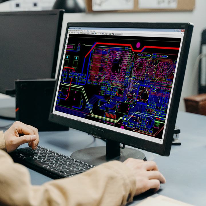
CAD schematic diagrams created to recognised industry standards, incorporating component footprint information and of course, the connectivity of the PCB. I can work from a hand-drawn sketch or any other input you wish to provide. Alternatively, you are welcome to submit your own CAD schematic or netlist.
Schematic symbols, parts and PCB footprint libraries are created for all components in the design, using the Bill of Materials (BOM)/parts list supplied.
Design of all types of printed circuit board – rigid and flexible, from single-sided through to multi-layer, incorporating through-hole and surface-mount components.
Existing PCB designs can be copied using a sample board (single or double-sided), Gerber files and paper or film plots of the separate layers.
Full electronic design service available. Please contact for details.
Step 1: As soon as I receive the information necessary to produce a quotation, the price and delivery for your PCB design is fixed.
Step 2: Working closely with you, paying particular attention to any special requirements, I design your board.
Step 3: You then have the opportunity to thoroughly check the layout – using paper check-plots, Gerber files, PDFs etc – whichever format you prefer.
Step 4: Any changes or adjustments are then made, before I submit a final set of check-plots or files for your approval.
Step 5: When you have confirmed that the layout is as required, I generate photo-plot and drill files, together with any other information or files required for the manufacture, assembly and testing of your board.
